High- speed PCB POFV insertion loss test
any high- speed PCB to be duly finagled to reduce excrescencies through rudiments analogous as impedance discontinuities in transmission lines, infelicitous plating of the through- hole interconnections or other losses of PCB signal integrity.
https://www.ymspcb.com/high-speed-pcb-pofv-insertion-loss-test-enepig-ymspcb.html
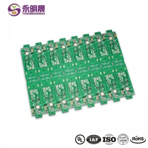
Parameters
Layers 8L High speed Material PCB
Board Thinkness1.6 mm
Base MaterialN4000-13SI
Min Holes0.2 mm
Minimum Line Width/ Clearance :0.075 mm/0.075 mm
Minimum Concurrence between Inner Caste PTH and Line :0.2 mm
Size :126.451 mm ×103.45 mm
Aspect Rate : 10 1
Face treatment : ENEPIG
Thing high speed material, insertion loss test, VIPPO
Differential impedance 1008Ω
ApplicationsNetwork dispatches
What is a High Speed PCB?
" High Speed"is generally interpreted to mean circuits where the length of the signal's rising or falling edge is lower than about one-sixth of the transmission line length lower also the transmission line length, also the transmission line length demonstrates lumped line behavior.
In a high speed PCB, the rise time is presto enough that the bandwidth for the digital signal can extend into the high MHz or GHz frequence. When this happens, there are certain signalling problems that will be noticed if a board is not designed using high speed PCB design rules. In particular, one might notice
1. Unacceptably large flash ringing. This generally occurs when traces are not wide enough, although you need to be careful when making your traces wider ( see the section on Impedance Contorl in PCB Design below). Still, you'll have large overshoot or undershoot in your signal transitions, If flash ringing is fairly large.
2. Strong crosstalk. As the signal speed increases ( i.e., as the rise time decreases), capacitive crosstalk can come fairly large as the convinced current exploits capacitive impedance.
3. Reflections off of automobilist and receiver factors. Your signals can reflect off of other factors whenever there is an impedance mismatch. Whether or not the impedance mismatch becomes important requires looking at the input impedance, weight impedance, and transmission line characteristic impedance for an interconnect. You can read further about this in the following section.
4. Power integrity problems ( flash PDN ripple, ground bounce,etc.). This is another set of necessary problems in any design. Still, flash PDN ripple and any performing EMI can be reduced significantly through proper stackup design and decoupling measures. You can read further about high speed PCB stackup design subsequently in this companion.
5. Strong conducted and radiated EMI. The study of working EMI problems is extensive, both at the IC position and the high speed PCB design position. EMI is principally a reciprocal process; if you design your board to have strong EMI immunity, also it will emit lower EMI. Again, ultimate of this boils down to designing the right PCB stackup.
High- frequency PCBs generally give a frequency range from 500 MHz to 2 GHz, which can meet the conditions of high- speed PCB designs, range, radiofrequency, and mobile operations. When the frequency is above 1 GHz, we can define it as high frequency.
The complexity of electronic factors and switches is continually adding presently and need hastily star flux rates. So, advanced transmission frequence are demanded. High- frequency PCBs help a lot when integrating special signal conditions into electronic factors and products with advantages like high effectiveness, and fast speed, lower attenuation, and constantdielectricproperties.Some considerations of high- frequency PCBs designs
High- frequency PCBs are mainly used in radio and high- speed digital operations, analogous as 5G wireless dispatches, automotive radar sensors, aerospace, satellites, etc. But there are multitudinous important factors to be considered when manufacturing high- frequency PCBs.
Multi-layered design
We generally usemulti-layered PCBs in high- frequency PCB designs. Multi-layered PCBs have assembly density and small volume, making them truly suitable for impact packages. Andmulti-layered boards are accessible to dock the connections between electronic factors and meliorate the speed of signal transmission.
Ground airplane designing is an important part of high- frequency operations because it not only maintains signal quality but also helps reduceEMIradiations.High frequency board for wireless operations and data rates in the upper GHz range have special demands on the material used
1. Shaped permittivity.
2. Low attenuation for effective signal transmission.
3. Homogeneous construction with low forbearance in insulation viscosity and dielectric constant. The demand for high- frequency and high- speed PCB products rises swiftly presently. As an educated PCB manufacturer, YMS is fastening on furnishing guests with reliable high- frequency PCB prototyping withhighquality.However, please feel free to communicate us, If you have any problems with PCB designing or PCB manufacturing.
To learn more, please click here:
YONGMINGSHENG TECHNOLOGY CO., LTD.


评论
发表评论